This blog post presents an accessible adaptation of my university seminar paper examining the architectural evolution of Google's Tensor Processing Units (TPUs). Based on peer-reviewed research and official technical documentation, it explores how Google revolutionized AI hardware design through three generations of domain-specific accelerators.
TL;DR
Google built TPUs to deliver predictable, energy-efficient performance on matrix-heavy ML workloads where CPUs/GPUs struggled. The architecture evolved from v1's INT8 inference to v2/v3's bfloat16 training at scale, then to v4+ with HBM, large pods, custom interconnects, and sparsity accelerators. If you train at scale or serve latency-sensitive models, TPUs can offer strong throughput and performance per watt.
The Catalyst: When General-Purpose Hardware Hit the Wall
In 2013, Google's capacity planning team delivered a sobering projection: if every Android user performed just three minutes of voice recognition daily, the company would need to double its entire datacenter infrastructure. This wasn't just a scaling challenge, it was an economic and environmental crisis in the making.
The root problem lay in the fundamental mismatch between AI workloads and general-purpose hardware. Neural network inference is dominated by dense matrix multiplications, but CPUs and even GPUs were designed for flexibility, not efficiency at this specific task. When Google tested NVIDIA's K80 GPU under real-world conditions with sub-10ms response time requirements, it performed only marginally better than a CPU because the strict latency constraints prevented effective request batching.
The features that make CPUs and GPUs excellent at general workloads, deep caches, complex instruction pipelines, and sophisticated branch prediction, were actually counterproductive for predictable, matrix-heavy AI inference tasks.
This realization sparked Google's bold decision to design custom silicon optimized specifically for neural network operations. The goal was ambitious: achieve a 10x improvement in cost-performance over GPUs while meeting stringent latency requirements. The timeline was equally aggressive, just 15 months from project initiation to datacenter deployment.
TPU v1: Redefining Inference Acceleration
Released in 2015, TPU v1 represented a radical departure from conventional processor design. Rather than pursuing general-purpose flexibility, Google's engineers focused ruthlessly on the operations that matter most for neural network inference.
Architectural Philosophy: Simplicity and Determinism
The 15-month development timeline forced crucial design decisions that ultimately became TPU v1's greatest strengths. Instead of complex out-of-order execution or sophisticated caching hierarchies, the team chose predictable, software-managed dataflow patterns that could guarantee consistent performance under strict latency requirements.
TPU v1 was implemented as a PCIe Gen3 x16 coprocessor card, allowing integration into existing server infrastructure without major datacenter modifications. The host CPU would compile entire neural network inference graphs into instruction sequences and stream them to the TPU, which would then execute autonomously with minimal further intervention.
The Heart of the Machine: Systolic Array Architecture
At TPU v1's core lies a 256x256 systolic array of 8-bit multiply-accumulate (MAC) units. Systolic arrays process data in synchronized waves: input activations flow from one direction, weights from another, and as these data fronts traverse the grid, they perform matrix multiplication with remarkable efficiency.
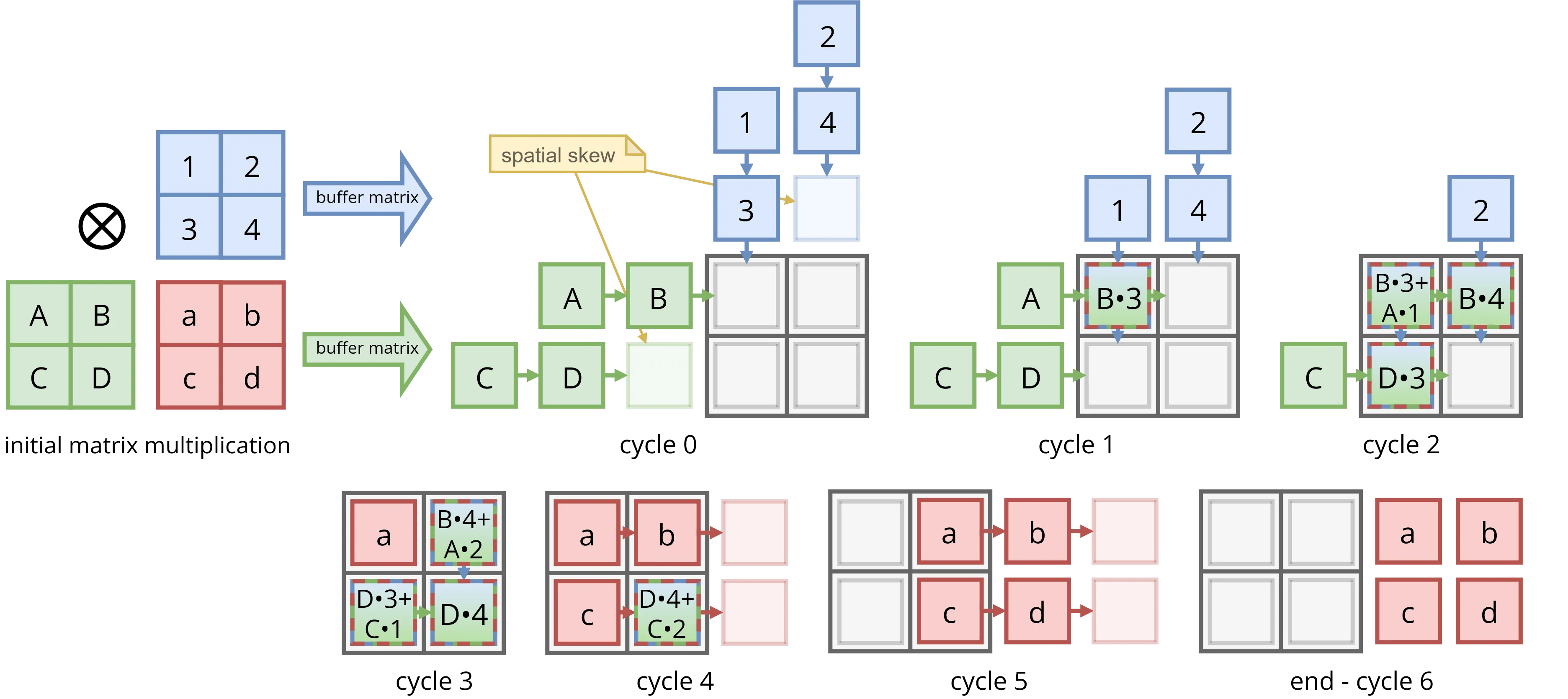
Once the pipeline fills, this array delivers 65,536 MAC operations per clock cycle. Running at 700 MHz, TPU v1 achieves approximately 92 TOPS of 8-bit integer performance, far exceeding what general-purpose hardware could deliver at the time.
Memory Without Caches: The Unified Buffer Approach
Perhaps TPU v1's most radical decision was eliminating hardware-managed caches entirely. Instead, it features a 24 MiB software-managed scratchpad called the Unified Buffer, occupying 29% of the die area. This design choice eliminated cache misses, unpredictable latencies, and complex coherence protocols, creating the deterministic execution model essential for meeting 99th-percentile response time requirements.
The data flow is elegantly simple: neural network weights stream from 8 GiB of on-card DDR3 memory into a weight FIFO buffer, while input activations stage in the Unified Buffer via DMA from host memory. The systolic array consumes data from both sources at a steady rate, with results flowing through activation functions and optional normalization before returning to the Unified Buffer.
Strategic Design Choices
Several key decisions shaped TPU v1's effectiveness:
8-bit Integer Arithmetic: By operating exclusively on quantized 8-bit integers with 32-bit accumulators, TPU v1 achieved 4x memory savings and significantly smaller, more power-efficient MAC units compared to floating-point alternatives. Google demonstrated that many neural networks could be quantized from 32-bit floats to 8-bit integers with negligible accuracy loss.
Deterministic Execution: Every aspect of TPU v1's design prioritized predictable latency over peak performance. This philosophical choice proved crucial for user-facing services where consistent response times matter more than maximum throughput.
Process Technology: Built on mature 28nm technology running at 700 MHz, TPU v1 achieved its gains through architectural innovation rather than aggressive process scaling, proving that smart design could outweigh raw transistor advancement.
Performance Results: Validating the Vision
TPU v1's real-world performance validated Google's architectural bet. On production inference workloads, a single TPU chip delivered 29.2x higher throughput than a contemporary Haswell CPU and 15.3x higher throughput than an NVIDIA K80 GPU. The efficiency gains were even more dramatic: 83x better performance-per-watt than the CPU and 29x better than the GPU.
More importantly, TPU v1 excelled under latency pressure. In a production service with a 7ms deadline, the Haswell CPU sustained only 42% of peak throughput and the K80 GPU managed 37%, forced to use small batches. TPU v1 maintained 80% utilization under the same constraints, demonstrating its architectural advantage for latency-sensitive applications.
Performance/Watt Comparison
Relative to CPU or GPU for various TPU generations
Limitations and Learning Opportunities
Despite its success, TPU v1 revealed important constraints. The primary bottleneck was memory bandwidth, DDR3's ~34 GB/s proved insufficient for many models. Google's analysis showed that a hypothetical "TPU v1 Prime" with GDDR5 memory would have tripled throughput and doubled efficiency, highlighting memory as the critical limiting factor.
The rushed development timeline also precluded sophisticated power management. At 10% utilization, TPU v1 still consumed 88% of peak power, poor energy proportionality that would be addressed in later generations.
Most significantly, TPU v1's integer-only arithmetic excluded it from training workloads, which require higher-precision floating-point calculations. This limitation would drive the fundamental changes seen in TPU v2.
TPU v2: Enabling the Training Revolution
By 2017, neural network training had become as computationally demanding as inference, if not more so. Training state-of-the-art models required days or weeks even on GPU clusters. TPU v2 represented Google's response: a ground-up redesign that could accelerate both training and inference at unprecedented scale.
bfloat16: Engineering the Perfect Compromise
The transition to training demanded floating-point arithmetic, but Google's engineers recognized that standard formats had limitations. IEEE 754 FP32 provides excellent precision but is computationally expensive, while FP16's limited 5-bit exponent often requires algorithmic workarounds like loss scaling to avoid numerical instability.
Google's solution was bfloat16 (bf16), a custom format that keeps FP32's 8-bit exponent for full dynamic range but reduces the mantissa to 7 bits. This design choice proved inspired: bfloat16 maintains the vast numerical range needed for training gradients while achieving the computational density of 16-bit arithmetic.

Architectural Evolution: From Single to Dual-Core
TPU v2 fundamentally restructured the processing architecture. Instead of one massive systolic array, it features two "TensorCores," each containing a 128x128 MXU and 16 MiB of dedicated vector memory. This dual-core design provides similar aggregate compute while improving memory bandwidth utilization and enabling more flexible workload mapping.
The memory subsystem received the most dramatic upgrade. TPU v2 replaced DDR3 with 16 GiB of High Bandwidth Memory (HBM2) delivering 700 GB/s, more than 20x the bandwidth of TPU v1. This eliminated the memory wall that had constrained the first generation and enabled the compute units to run at full efficiency across a much broader range of models.
Scaling to Supercomputer Dimensions
Training large models requires distributed computation across many accelerators. TPU v2 was designed from the ground up for this reality, featuring four custom Inter-Core Interconnect (ICI) links, each providing 496 Gbit/s of bandwidth. These enable chips to be connected in a 2D torus topology for efficient all-to-all communication.
A full TPU v2 "Pod" comprises 256 chips arranged in a 16x16 torus, delivering 11.8 PetaFLOPS of aggregate performance. At this scale, the interconnect becomes as important as individual chip performance, Google's custom topology ensures that communication patterns common in distributed training can proceed with minimal bottlenecks.
Hardware-Software Co-Design: The XLA Advantage
TPU v2's hardware capabilities are amplified by sophisticated software. The XLA (Accelerated Linear Algebra) compiler performs whole-program optimization, analyzing entire neural network training graphs and generating highly optimized code for the TPU's unique architecture.
XLA's impact extends far beyond initial deployment. Through compiler optimizations alone, TPU performance on MLPerf training benchmarks improved by a median factor of 2.1x over six months, demonstrating how co-designed software can unlock hardware potential long after silicon fabrication.
Less publicized at the time, TPU v2 quietly incorporated a set of "SparseCores" for accelerating the sparse operations common in recommendation models, a feature Google wouldn't reveal publicly until the TPU v4 paper.
TPU v3: Doubling Down on Scale and Performance
Released in 2018, TPU v3 represented a strategic evolution rather than a revolutionary redesign. Google's engineers took the proven v2 architecture and systematically enhanced every component to meet the growing computational demands of increasingly complex neural networks.
Architectural Refinements
The most significant change in TPU v3 was doubling the number of matrix units per TensorCore from one to two, giving each chip four 128x128 MXUs total. Combined with a clock speed increase to 940 MHz, this delivered 123 TFLOPS of bfloat16 performance per chip, a 2.7x theoretical improvement over v2.
Memory capabilities scaled proportionally: HBM2 capacity doubled to 32 GiB per chip with bandwidth increased to 900 GB/s. The Inter-Core Interconnect also received a 32% bandwidth boost to 656 Gbit/s per link, ensuring communication could keep pace with the enhanced compute capabilities.
Despite doubling the MXU count, TPU v3's die grew by only 6% compared to v2. This efficiency came from design experience, the team had learned to optimize floorplans and minimize wasted silicon area, demonstrating the value of iterative architectural refinement.
Supercomputer-Scale Performance
TPU v3 expanded maximum pod size to 1024 chips, four times larger than v2 pods. A fully configured TPU v3 pod delivers over 126 PetaFLOPS while maintaining 96-99% linear scaling efficiency on production workloads. This near-perfect scaling at thousand-chip scale represents a remarkable achievement in distributed system design.
The increased performance density came with thermal challenges. TPU v3's 450W TDP necessitated liquid cooling systems, air cooling could not handle the heat density in datacenter racks. This transition reflected the ongoing tension between performance and practical deployment constraints.
"What You Train Is What You Serve"
TPU v3 reinforced Google's "WYTIWYS" (What You Train Is What You Serve) philosophy. Unlike workflows that require separate quantization steps for inference deployment, TPU v3 uses bfloat16 for both training and serving. This eliminates potential accuracy degradation from format conversion and simplifies the machine learning pipeline.
Performance results validated this approach. On the LSTM0 benchmark, TPU v3 achieved 45ms inference latency, faster than even the inference-optimized TPU v1, which required 122ms for the same task. This demonstrated that the training-focused v2/v3 architecture could excel at inference while maintaining numerical consistency with training.
Modern TPU Evolution (v4-v7): Pushing the Boundaries
The architectural principles established in TPU v1-v3 continue evolving in subsequent generations, each addressing new challenges in AI computation at ever-greater scale. While detailed academic analysis exists primarily for the first three generations, official technical announcements provide insight into Google's continued innovation.
TPU v4: Optical Interconnects and Specialized Acceleration
TPU v4, released in 2020, achieved a 2.1x performance increase and 2.7x improvement in performance-per-watt over v3. Each chip delivers 275 TFLOPS of bfloat16 performance with 32 GiB of HBM providing 1.2 TB/s of bandwidth. However, v4's most significant innovations extend beyond raw compute metrics.
The introduction of Optical Circuit Switches (OCS) enables dynamic reconfiguration of the 3D torus interconnect, improving fault tolerance and allowing specialized network topologies for different communication patterns. This flexibility becomes crucial as pod sizes scale to 4096 chips and beyond.
The v4 paper also publicly revealed TPU's dedicated "SparseCores", specialized processors for the sparse operations common in recommendation systems and embedding-heavy models. Present since v2, they accelerate Deep Learning Recommendation Models by 5-7x while consuming only about 5% of die area and power, underscoring the value of heterogeneous acceleration within domain-specific architectures.
TPU v5 Family: Bifurcating for Efficiency and Performance
Disclaimer: For TPU v5 and later (including v5e/v5p, v6e, and v7), specifications and performance figures referenced here are based on Google's public claims and announcements, not peer-reviewed scientific papers.
With TPU v5, Google formalized a two-track approach addressing different market segments and use cases:
TPU v5e (Efficient): Designed for cost-conscious deployments, delivering 197 TFLOPS with 16 GB of HBM and 0.82 TB/s bandwidth. This variant targets organizations requiring solid ML performance without premium pricing.
TPU v5p (Performance): Built for maximum throughput at scale, offering 459 TFLOPS with 95 GB of HBM at 2.8 TB/s bandwidth. Pods scale to 8,960 chips with 4.8 Tb/s bisection bandwidth, targeting the largest training workloads and most demanding inference applications.
TPU v6e "Trillium": Efficiency Breakthrough
TPU v6e represents a significant advancement in the efficiency-focused line, achieving 918 TFLOPS per chip, nearly doubling v5e performance. Memory capacity increased to 32 GB with 1.64 TB/s bandwidth, while interconnect bandwidth more than doubled. Most importantly, v6e delivers 67% better energy efficiency compared to v5e, making it highly attractive for large-scale deployments where power consumption directly impacts operational costs.
TPU v7 "Ironwood": The Memory-Centric Future
Announced for 2025, TPU v7 addresses one of the most pressing challenges in modern AI: memory capacity. With 192 GB of HBM per chip running at 7.4 TB/s bandwidth, v7 can accommodate much larger models on-chip without constant data streaming from external storage.
The compute capability scales to match: over 4.6 PFLOPS per chip represents a 5x increase over v6e. However, the real innovation lies in achieving this performance while targeting 2x better performance-per-watt, continuing the trend of making each generation more energy-efficient even as absolute performance scales dramatically.
TPU Evolution: Specifications at a Glance
| Generation | Peak Compute | Precision | Memory / Bandwidth | Interconnect | Max Pod Size | Key Features |
|---|---|---|---|---|---|---|
| v1 | 92 TOPS (8-bit) | INT8 | 8 GiB DDR3 / 34 GB/s | N/A | Single chip | Inference-only, PCIe card, 75W TDP |
| v2 | 46 TFLOPS (bfloat16) | bfloat16 | 16 GiB HBM2 / 700 GB/s | 4× ICI @ 496 Gbit/s | 256 chips (11.8 PFLOPS) | Dual TensorCores, training capable |
| v3 | 123 TFLOPS (bfloat16) | bfloat16 | 32 GiB HBM2 / 900 GB/s | 4× ICI @ 656 Gbit/s | 1024 chips (126 PFLOPS) | Liquid cooling, 4× MXUs per chip |
| v4 | 275 TFLOPS (bfloat16) | bfloat16 | 32 GiB HBM / 1.2 TB/s | OCS + 3D torus | 4096 chips | Optical interconnect, SparseCores since v2 |
| v4i | ~275 TFLOPS (bfloat16) | bfloat16 | 32 GiB HBM / 1.2 TB/s | N/A | Single chip | Inference-optimized, air-cooled |
| v5e | 197 TFLOPS (bfloat16) | bfloat16 | 16 GB HBM / 0.82 TB/s | Standard | Variable | Cost-efficient training/inference |
| v5p | 459 TFLOPS (bfloat16) | bfloat16 | 95 GB HBM / 2.8 TB/s | 4.8 Tb/s bisection | 8960 chips | High-performance training |
| v6e | 918 TFLOPS (bfloat16) | bfloat16 | 32 GB HBM / 1.64 TB/s | >2× v5e | Variable | 67% better efficiency vs v5e |
| v7 | >4.6 PFLOPS (bfloat16) | bfloat16 | 192 GB HBM / 7.4 TB/s | TBD | TBD | 2× perf/W vs v6e (announced 2025) |
Architectural Paradigms: GPU vs FPGA vs TPU
The success of TPUs has catalyzed broader industry adoption of domain-specific accelerators, but different architectural approaches serve distinct use cases. Understanding when to choose GPUs, FPGAs, or TPUs requires analyzing the fundamental trade-offs between programmability, latency, throughput, and efficiency.
The Latency-Throughput Spectrum
Each architecture optimizes for different points on the latency-throughput spectrum:
FPGAs excel at ultra-low latency: Microsoft's Brainwave project demonstrated that FPGAs can achieve sub-4ms inference latency on complex models by extracting fine-grained parallelism from single requests. The Hierarchical Decode and Dispatch mechanism can expand one instruction into over 7 million primitive operations without requiring batching. This makes FPGAs ideal for real-time applications where individual request latency matters more than aggregate throughput.
TPUs and GPUs optimize for batched throughput: Both architectures achieve peak efficiency with larger tensor operations that keep their massive parallel compute arrays busy. TPUs gain an additional advantage through deterministic execution, by eliminating cache misses and other sources of latency variance, they can operate closer to peak throughput even under strict 99th-percentile latency constraints.
Flexibility vs Specialization Trade-offs
The architectural spectrum reflects different philosophies about adaptability:
GPUs provide maximum programmability: NVIDIA's CUDA ecosystem enables rapid prototyping and supports diverse model architectures. This flexibility makes GPUs essential for research environments where new techniques emerge rapidly. However, general-purpose design incurs overhead that specialized architectures avoid.
FPGAs offer reconfigurable specialization: The ability to synthesize custom datapaths and numerical formats (like Microsoft's Block Floating-Point) provides a middle ground between flexibility and efficiency. FPGAs can adapt to new model architectures through hardware reconfiguration rather than software changes alone.
TPUs achieve efficiency through co-design: While hardware is fixed at fabrication, the tight integration with XLA compiler enables continued optimization. Google demonstrated median 2.1x performance improvements on MLPerf benchmarks through software optimization alone, showing that ASIC platforms can evolve through compiler advancement.
AI Accelerator Architecture Comparison
| Attribute | GPU (e.g., NVIDIA Volta) | FPGA (e.g., MS Brainwave) | TPU (Google v1-v3) |
|---|---|---|---|
| Architecture | Programmable parallel processor | Reconfigurable logic | Domain-specific ASIC |
| Primary Strength | Flexibility and research velocity | Ultra-low latency (batch-of-1) | Throughput and efficiency at scale |
| Compute Primitive | SIMT cores (thread-based) | Matrix-vector operations | Systolic matrix-matrix arrays |
| Memory System | Hardware caches + HBM | Software-managed SRAM | Software-managed SRAM + HBM |
| Scaling Model | NVLink + InfiniBand | Network-attached services | Custom torus/OCS pods |
| Best Use Cases | Diverse ML workloads, research | Latency-critical inference | Large-scale training, batched inference |
System-Level Integration Strategies
Beyond individual chip performance, these architectures differ fundamentally in system-level integration:
Disaggregated vs. Integrated Scaling: Microsoft's Brainwave treats FPGAs as network-attached "hardware microservices," enabling flexible resource allocation. In contrast, TPU Pods are purpose-built supercomputers with custom torus interconnects optimized for specific communication patterns in distributed training.
Communication Architecture: GPUs rely on established standards like NVLink and InfiniBand for inter-device communication. TPUs use custom Inter-Core Interconnect (ICI) and Optical Circuit Switches (OCS) designed specifically for ML workload communication patterns. This specialization enables near-perfect linear scaling to 1000+ chips but reduces flexibility for other workload types.
Impact and Future Directions
Industry Transformation
The TPU project's success validated domain-specific architecture as a viable alternative to general-purpose scaling. This has triggered industry-wide innovation: AWS developed Inferentia and Trainium, Microsoft created Brainwave, Intel introduced Gaudi, and NVIDIA enhanced their GPUs with specialized Tensor Cores. The competitive landscape now features diverse approaches to AI acceleration rather than reliance solely on general-purpose processors.
Architectural Lessons and Principles
Several key principles emerge from the TPU v1-v3 evolution:
Hardware-software co-design amplifies benefits: The tight integration between TPU hardware, TensorFlow framework, and XLA compiler enabled optimizations impossible with generic interfaces. This co-design approach has become standard practice across the industry.
Deterministic execution enables predictable performance: By eliminating sources of latency variance like cache misses and complex scheduling, TPUs can maintain high utilization under strict tail-latency requirements. This predictability proves crucial for user-facing AI services.
Memory architecture evolution follows compute scaling: The progression from DDR3 (v1) to HBM2 (v2/v3) to massive HBM capacity (v7) reflects the growing importance of memory bandwidth and capacity as model sizes increase exponentially.
Future Challenges and Opportunities
The TPU roadmap illuminates several key trends shaping AI hardware's future:
Memory-centric design: TPU v7's 192 GB of on-chip memory addresses the reality that model parameters are growing faster than memory capacity. Future architectures will likely prioritize memory systems as much as compute units.
Energy efficiency as first-class concern: Each TPU generation improves performance-per-watt even as absolute performance scales dramatically. With training costs reaching millions of dollars and significant environmental impact, efficiency improvements become as important as raw performance gains.
Heterogeneous acceleration: Future designs will likely incorporate diverse accelerators optimized for different operation types within AI workloads.
The TPU story demonstrates that when conventional approaches reach their limits, focused architectural innovation can achieve breakthrough results. The key insight isn't just building faster chips, it's co-designing hardware and software together while ruthlessly optimizing for the workloads that matter most.
Conclusion: Lessons for the Future of AI Hardware
Google's TPU journey from v1's inference-focused design to v7's massive-memory architecture illustrates how domain-specific innovation can overcome seemingly insurmountable scaling challenges. Faced with exponential growth in AI computational demands, Google chose specialization over generalization, and achieved performance improvements that would have been impossible through traditional scaling approaches.
The architectural principles established in TPU v1-v3 continue driving innovation across the industry. Systolic arrays optimized for matrix operations, software-managed memory hierarchies that eliminate unpredictable latencies, custom interconnects designed for ML communication patterns, and tight hardware-software co-design have become standard practices in AI accelerator development.
Perhaps most importantly, the TPU project demonstrated that breakthrough performance requires more than faster transistors or higher clock speeds. The most significant gains come from understanding your workload deeply, designing hardware specifically for those patterns, and co-evolving software to maximize the architecture's potential. As AI continues pushing the boundaries of computation, this philosophy of focused, co-designed specialization will likely define the next generation of breakthrough architectures.
Explore Further: Academic Deep Dive
This blog post provides an accessible overview of Google's TPU architecture evolution. For readers interested in deeper technical analysis, including detailed performance modeling, comparative benchmarks, and architectural trade-offs, my complete seminar paper offers comprehensive academic treatment with full citations to primary research.
Note: This paper was submitted as part of university coursework and has not undergone independent peer review.
Download Full Academic Paper (PDF)